In case of signal transmission among various cable applications, it is important to prevent from getting mixed with noise and to reduce affection to external environment in addition to fast transmission to the atmost without distortion nor large attenuation, so that various kinds of noise countermeasure technics have been developed from old time.
Basical screen (shield) technique is tried to be explained hereafter. Please note that there is reversibility between screen (shield) that protects from noise come from out side and EMI (Electromagnetic Interference) that interferes outside from noise source cable. Therefore, shield technique and interfering control technique become exactly same. In other words, it is same to think about either way. (Note: 1)
The most important point when think about screen (shield) and or countermeasure against noise is to grasp the noise mixing mechanism exactly (accurately) which is comprised of different mechanism. This different mechanism are following based on electric circuit technique.
| Coupling Type | Circuit Element | Noise Source | Coping Method |
|---|---|---|---|
| Conductive Coupling | Common Impedance | Current or Voltage Source | Circuit Isolation |
| Capacitive Coupling | Mutual Capacitance | Voltage Source | Electrostatic Shield |
| Inductive Coupling | Mutual Inductactance | Current Source | Cancelling |
| Electromagnetic Wave | Radiation Field | Electricmagnetic radiation/reception | Electromagnetic Shield |
All of these property are undescribed part in electric circuit and they must be paid carful attention that they are all different physical mechanism so that countermeasure method has to become quite different.

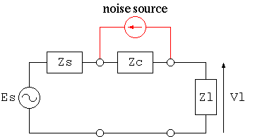
Fig. 1: Common Impedance Coupling
When multiple circuits such as earth wire, earth plate and or printed circuit board etc., share a same circuit element, noise is generated by flown electric current from other circuits. In case of direct current or low frequency, it is easy to lower the value of common impedance coupling by increasing earth conductor size. However, in case of high frequency, it becomes not negligible because common impedance caused by inductance element increases proportionally to frequency.
Therefore, basical countermeasure becomes isolation of circuits so that earth wire is separated with each circuit and made into single point ground so that GND potential is fixed. This method becomes principle.
Interesting point that happens with cable peculiarly among conductive coupling is the case that external conductor of a coaxial cable becomes common impedance.
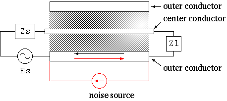
Fig. 2: Transfer Impedance of a Coaxial Cable (Cross Section of a Coaxial Cable)
It is common case that electric current flows into external conductor of coaxial cable from other circuit as shown in figure 2. External conductor of coaxial cable is usually grounded so that it is difficult to get rid of loop combined with other earth line, and even though this external conductor is not included in a loop, if there is electromagnetic wave in its surrounding, external conductor works (performs) as an antenna so that electric current flows by electromotive force caused by received electromagnetic wave. Please remember that long cable becomes a good antenna.
However, as the frequency of transmitted signal and noise increases, majority of transmitted signal flows inside of external conductor and noise current flows outside of external conductor by skin effect so that this common impedance circuit is automatically separated.
The following formula is useful to know how deep high frequency current flows in the surface of conductor, which is called as skin depth.
  δ = sqrt(2 / (ω * μ * σ))
  hereby,
	δ = skin depth (m) ..
             In case of electrolytic cathode copper, it is 8.46e-2/sqrt(f)
	ω = angular frequency (rad/s)
	   = 2 * π * f
	f = frequency (Hz)
	π = 3.14519265..
	μ = magnetic permeability of conductor (H/m) ..
             In case of nonferrous metal, it is 4e-7*π
	σ = conductivity (S/m) ..
	σ = conductivity (S/m) ..
             In case of electrolytic cathode copper, it is 5.8e7
Surprisingly, resistance value of 1.6*δ thickness cylindrical conductor
and same overall diameter of columnar conductor does not differ more than
several percentage.
For example, δ of electrolytic cathode copper at 100 MHz is 8.5 μm,
so how this circuit isolation mechanism is efficient.
Of course, as flown frequency becomes low, branched current from noise into transmission line increases, it is necessary to know its frequency characteristic of this mechanism and this indicator so called Transfer Impedance is used for this purpose which is defined as follows:
  Zt = Vt / I
  hereby,
	Zt = transfer impedance (Ω)
	Vt = generated voltage on the surface of external conductor per unit length (V/m)
	I =  current that flows internal conductor (A)
This is considering that how much signal current affects to other circuits so that thinking it upside down. However, it does not matter because there is reversibility between them, and it makes us not necessary to care for other circuits by this way of definition.
In case external conductor structure is cylindrical, current distribution can be shown (expressed) by Bessel function so that Zt can be obtained analytically. And, in case thickness of external conductor is small enough compared to its internal (inside) diameter, it becomes as follows:
  Zt / Rdc 〜 p * t / sinh(p * t)
  hereby,
	t = thickness of external conductor (m)
	Rdc = DC resistance of external conductor (Ω)
	p = (1 + j) / δ
	j = sqrt(-1)
	δ = skin depth (m) ..
             In case of electrolytic cathode copper, it is 8.46e-2/sqrt(f)
If frequency is zero, Zt is equal to DC resistance naturally, and as it becomes
high, this value decreases swiftly so that crosstalk with external circuit
decreases.
In case of braided shield structure, since inside electromagnetic field leaks through openings between conductors, mutual capacitance and mutual inductance between internal conductor and the surface of external conductor are generated so that transfer impedance is added proportionally to frequency. Zt is increased proportionally to frequency from around several MHz normally. As countermeasure against it, polyester-film-reinforced aluminum foil is inserted underneath the braided shield in geneal. It gives satisfactory result up to GHz bandwidth, although cable lose flexibility.
Another interesting method as a countermeasure against conductive coupling for a coaxial cable is to wind cable itself over a ferrite core so that self-inductance of the noise circuit including external conductor increases, which is called Coaxial Choke. In this case, inductance consists of external conductor and other conductor circuit can be increased without affecting electrical characteristic between internal conductor and external conductor circuit of the coaxial cable, therefore this method can reduce noise current only without affecting signal circuit. This is the same idea as Common Mode Choke that is often used for countermeasure against common mode noise.
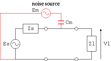
Fig. 3: Capcitive Counpling by mutual capacitance
Capacitive coupling is caused by electrostatic induction by electric field generated by voltage generator that arises noise. As an electric circuit, current flows into signal circuit from other circuit through (via) mutual capacitance Cm. Cm is normally considerably small so that this impedance is large, therefore noise source becomes constant current source for load Zl side. Therefore, when the impedance of the signal circuit is high (large), it becomes problem.
There is an extremely effective method called Electrostatic Shield against capacitive coupling in addition to (other than) separating (setting apart) from high voltage generator and reducing impedance Zs of the signal circuit.
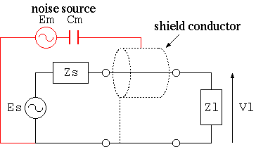
Fig. 4: Electrostatic Shield
This method is to bypass noise current by enclosing signal line with conductor so-called electrostatic shield and connecting to GND. Since impedance of this electrostatic shield conductor is extremely low compared to capacitance between signal conductor and electrostatic shield conductor, this baypass mechanism functions extremely effective in deed. Of course, if there is openings in this shield conductor, mutual capacitance between signal conductor and noise generator is arised so that noise current is increased at high frequency.
Braiding, serving (spiraling) and conductive tape are usual shield structure used for wire and cable. Conductive tape without any opening is the most cost effective structure, but it's weak point is inflexibility. Serving (spiraling) is to wind many annealed copper wires in a row (lay flat), so it becomes flexible and generated openings between neighbour conductor is much less than braiding structure, but it's weak point is uneasy production process and possibility of increased cross-talk at high frequency in case of one layer structure. Brading structure has good balance of flexibility and shielding effect so that this method has been used for varied cable structures from coaxial cable's external conductor up to overall shield for multicore cables from the old time. For counter- measure against openings between conductors of braiding structure at high frequency, double brading structure or combination of brading structure and polyester-film-reinforced aluminum foil are often used.
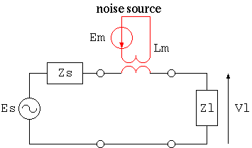 Fig. 5: Coupling by Mutual Inductance
Electromagnetic coupling is generated when magnetic flux generated by noise source electrical current interlinks with signal circuit where electromotive force is generated by magnetic flux so that this coupling is mutual inductance coupling in terms of a circuit. In this case, noise becomes constant voltage supply so that affection by noise becomes larger at low impedance circuit and even though feed end side (transfer end side - sending end side) of a signal line is shorted, noise can be appeared at load side. In other words,
If magnetic flux generated by noise source electrical current does not interlink with signal circuit, it is not affected by it, so that we want to think about magnetic shielding, however, there is not any appropriate magnetic material. Therefore, the following two methods are used for counter-measure against inductive coupling by this reason.
Strategy of the latter method is to utilize existence of plus and minus sign in mutual inductance unlike mutual capacitance, combining same magnitude with opposite sign mutual inductance to deprive (eliminate) mutual inductance in a whole circuit. It functions well at relatively low frequency range. However, when frequency rises up high, it does not function well because of increased affection by stray capacitance.

Fig. 6: Cancellation of Electromagnetic Coupling by twisted pair structure (Arrow shows directon of electromotive force by noise)
The most often used method is twisted pair structure which is to twist two conductors of a round trip of transmission line at fixed pitch so that direction of electromotive force caused by interlinkage magnetic field is inverted at every pitch, so it can be canceled sequentially. As in terms of a circuit, mutual inductance becomes zero by inverting plus and minus of mutual inductance with noise source at every pitch when it is contour integrated. Otherwise interlinked magnetic field is same largeness between neighbour pitch, it does not function. However, interlinkage magnetic field between neighbour pitch can become very close to zero by making twisted pitch short and distance of two conductors very close. It costs rather high to twist at short pitch, on the other hand there are many advantages such as not sacrificing flexibility, so this technique is extensively used.
Besides, though it is touched later on once again, in case a twisted pair is used for balanced transmission line, capacitance coupling with outside induction voltage source becomes almost same strength so that capacitance coupling is also canceled at the same time as well as electromagnetic coupling, so effectiveness of two birds with one stone could be gained. The very reason why lan cable can be used without overall shield lies in this point.
There are some othe mthods to cancel electromagnetic coupling, star-quad configuration is often used for a microphone cable that is used at a close distance from a large current dimmer.

Fig. 7: Cancellation of electromagnetic coupling by star-quad connection
Idea of this method is to short opposite (diagonal) conductors of a four conductor cable to use it as one go and return conductor, considering X-direction of magnetic flux in Fig. 8 cross section, direction of induced electromotive force generated in conductor 1 and 2 loop and that in conductor 3 and 4 are reversed so that both induced electromotive forces are canceld respectively.
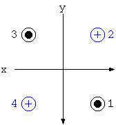
Fig. 8: Cross section of star-quad connection and direction of induced electromotive force
This canceling mechanism becomes the same with Y-direction, therefore, canceling is done in a small geometric scale as about twice as the insulation thickness so that it becomes considerablly advantageous against non-homogeneity (ununiformity) of induction field.
Twisted-pair-pitch is about 20 times of overall diameter of insulation even though it is twisted densely, fineness of cancelling mesh of a quad configuration exceeds roughly twenty times of star-quad structre so that it can be expected over 26 dB improvement.
This conductor structure and combination of conductors is same as phantom circuit of a cabled telephone line, however, in case of cabled telephone line (phantom circuit), diagonal pairs are used independently and they are also used for parallel connection as the third line. This technique secures three circuits by two twisted pair cables preventing from large cross-talk so that it contributes cost down. In case of quad structure of a microphone cable, it is quite different idea because its strategy is to reduce mutual inductance by peripheral circuits being aware of cost-up.
Furthermore superior structure with regard to canceling function is a coaxial cable. As long as linkage magnetic flux is symmetry about its centre conductor, reversed direction electromotive force is generated at both side of the outernal conductor of the coaxial cable so that essentially perfect induced electromotive force cancellation is taken place.
In case of a coaxial cable made of perfect conductor whose electrical resistivity is zero, electromagnetic field inside its cable does not leak outside of a cable, it can create an independent space from any other circuit in terms of electromagnetic field, therefore, it could be understood that there is no mutual inductance with any outside circuits, considering reversibility.
Both of electric field caused by capacitive coupling and magnetic field caused by electromagnetic (inductive) coupling becomes weak inversely proportional to square of distance from the source, therefore affection beomes low sharply as it parts from the noise source. In other words, strategy to set a signal circuit apart from a noise source is very effective, so shielding and or canceling technique is utilized when it (separation) cannot be used.
On the other hand, electromagnetic wave does not attenuate inversely proportional to square of distance from the source different from sole electric field or megnetic field, but it attenuates inversely proportional to distance from the source so that it affects to the distance up to extremely far away. This nature is utilized for radio communication such as broadcasting.
This situation can be understood quite well by observing a generated electromagnetic field inside small loop or infinitesimal dipole whose circuit size is small enough compared to wavelength. For example, centre of infinitesimal loop is set to be origin of x-y-z coordinates, and loop plane is set on x-y plane, electromagnetic field is expressed as shown below:
  Hr = I*A/λ *(j/r^2 + λ /2/π/r^3)*cos(σ)
  Hσ = &pi*I*A/ λ^2/r*sqrt(1 - (/2/mbda;π/r)^2 + ( λ/2/π/r)^4)*sin(σ)
  Eφ = Z0*π*I*A/λ^2/r*sqrt(1 + (λ/2/π/r)^2)*sin(σ)
  hereby,
	r = distance from the centre of infinitesimal loop (m)
	σ = angle between straight line connecting origin and observation point and Z-axis (rad)
	Φ  = angle between straight line connecting origin and observation point and X-axis (rad)
	Hr = magnetic field at straight line connecting origin and observation point direction (A/m)
	Hσ = magnetic field at surface direction including straight line connecting origina and observation point
              and Z-axis (A/m)
	EΦ = electric field at X-Y-axis surface direction (at loop plane) (V/m)
	A = area (square measure) of loop (m^2)
	I = electrical current flow in loop (A)
	λ = wavelength (m)
	   =  3e8/f
	f = frequency (Hz)
	r = daistance between centre of loop and observation point (m)
	Z0 = free space impedance (Ω)
	   = 120*π = 377
	j = sqrt(-1)
Considering X-Y-axis surface (loop plane) whose electromagnetic field is large, it is separated into the following
two cases:
      H = I*A/4/π/r^3  (A/m)
      E = Z0*I*A/2/λ/r^2  (V/m)
      H = π*I*A/λ^2/r  (A/m)
      E = Z0*π*I*A/^2mbda;/r  (V/m)
In case of tying infinitestimal loops into a row, electrical current component crossing at right angle against the line cancels each other so that it becomes zero and it becomes same as parallel two conductor transmission line, therefore, it becomes same transmission line characteristics as parallel two conductor cable as it is, so electric field at far area by round trip current of small conductor distance parallel two conductor cable accords with the value replacing area (square measure) of round trip conductors with that of infinitestimal loop as shown below.
  E = 120*π^2*I*s*h/λ^2/r  (V/m)
  hereby,
	E = electric field at far area by round trip current of a parallel two conductor configuration (V/m)
	I = current (A)
	s = length of a parallel cable (m)
	h = distance between two conductors of a parallel cable (m) .. h << λ
	λ = wavelength of round trip curremt of a parallel cable .. 3e8*coefficient of velocity/frequency
	r = distance between central axis of a parallel cable and observation point (m)
Hereafter, when centre of infinitestimal dipole is set origin of Y-axis of x-y-z coordinates, electromagnetic field is expressed as shown below:
  Er = 60*I*s*(1/r^2 - j*λ/2/π/r^3)*cos(σ)  (V/m)
  Eσ = Z0*I*s/2/π/r*(1 - (λ/2/π/r)^2 + (λ/2/&pi/r)^4)*sin(σ)  (V/m)
  H&Phi = I*s/2/λ/r*(sqrt(1 + (λ/2/π/r)^2)*sin(σ)  (A/m)
  hereby,
	I = current flows in dipole (wire) (A)
	s = length of dipole (wire) (m)
Considering X-Y-axis surface whose electromagnetic field is large, it is separated into the following two cases:
      H = I*s/4/π/r^2  (A/m)
      E = Z0*L*s*λ/8/π^2/r^3  (V/m)
      H = I*s/2/λ/r  (A/m)
      E = Z0*I*s/2/λ/r  (A/m)
Difference between infinitestimal loop and infinitestimal dipole is deeply understood when comparing ratio of electric field and magnetic field E/H (Ohm), in other words, comparing wave inpedance (surge impedance - characteristic impedance). In case of infinitestimal dipole, wave impedance is extremely high at short distance, and it becomes smaller as distance becomes larger and finally it accords with wave impedance of free space (120*π) at far field. On the other hand, in case of infinitestimal loops, wave impedance at short distance is very low on the contrary, and it increases as distance becomes larger and finally it accords with wave impedance of free space (120*π) at far field. Therefore, in either way, as long as it is apart from origin (source) of electromagnetic wave far away, both segment accord with each other because of under control of free space in either way. In other words, they show antithetical characteristic at short distance.
When considering coupling with external circuit, although largeness of electric field and magnetic field is reversal between infinitestimal loop and infinitestimal dipole at short distance, it is far from wave impedance at free space in either way, efficiency as antenna is not good because of mismatching with free space impedance.
The other way, as area (square measure) of loop and or length of dipole becomes close to 1/4 wavelength of high frequency current, wave impedance at adjacent area becomes close to the wave impedance at free space, so that it functions as antenna effectively. Since wire and cable are long, it is common that shield acts as an antenna. Therefore, commonly ferrite beads are inserted at a certain interval as its countermeasure to prevent from emission or making hard to flow receiving current.
Only method to screen (shield) from electromagnetic wave is to wrap a whole circuit with high conductivity case (chassis), joint utilizing electromagnetic wave reflection generated between outernal space and case and attenuation by eddy current loss generated inside case material.
Reflection loss among these two factors is determined by ratio of wave impedance between free space and inside conductor, which is as shown below:
  R = 20*log10(sqrt(σ/(ω*μ*ε ))/4)
  hereby,
	R = reflection loss (dB)
	σ = conductivity (S/m)
	   = σs * 5.80e7 (S/m)
	σs = conductivity (specific conductivity against cathode copper)
	*mu; = magnetic permeability (H/m)
	   = μs * 4e-7 * π
	μs = relative permeability
	ε  = dielectric constant (F/m)
	   = εs * 1e7 / (4 * π * c^2)
	ε s = relative permittivity
	c = 299,792,458 m/s (velocity of light in a vacuum)
	ω = angular velocity (rad/s)
	   = 2 * π * f
	f = frequency (Hz)
Attenuation loss is determined by skin depth and thickness of used material, which is as shown below:
  A = 20 * log10(exp(t / δ))
  hereby,
	A = attenuation loss (dB)
	t = thickness of shielding material (m)
	δ = skin depth (m)
Total shielding effect is sum of reflection loss and attenuation loss, and reflection loss is decreased inversely proportional to the square root of frequency, but attenuation loss radically increases at high frequency so that this mechanism functions effectively at high frequency. However, if there is a hole inside case, electromagnetic wave leaks through it, it becomes major problem how to take measure against openings.
Moreover, in case of electric field, reflection at exterior surface of shield material is large, so that attenuation loss effect becomes secondary. On the other hand, in case of magnetic field, reflection at interior surface of shield material is large so that attenuation loss inside becomes more important, because of limitation of available material it is hard to realize large attenuation. In any case, it can be understood that high conductivity material is required for this purpose.
Also, as a counter-measure against EMI (Electro-Magnetic Interference), because distance between shield and object circuit is reversal, it must be paid attention that far field must be considered in case of shield (screen), and adjacent area must be considered in case of EMI.
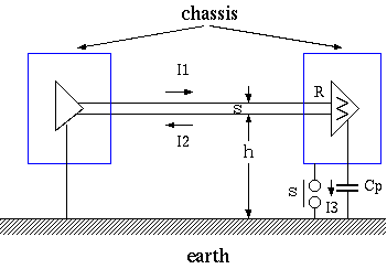
Fig. 9: Common-mode current (i3) - Impedance of Cp is low because of high frequency
When considering electromagnetic field generated by infinitestimal loop and or infinitestimal dipole, it is understood that the most efficient method is to make the circuit size small enough comparing wavelength. However, in case of transmission by cable, because length of wiring is long, in case of single end (unbalanced) transmission, use coaxial cable or utilize twisted pair cable reducing loop area to reduce current flow into ground (earth) as its home. Commonly used fundamental countermeasure is to let it differential circuit (balanced circuit) and use twisted pair cable so that signal current won't flow through ground (earth) in principle. Nevertheless, there remain unbalanced part of a circuit somewhere, part of signal current will flow through ground (earth), in other words, Common Mode component has to be generated.
Because area where common mode current flows is extremely large, even though it is a minute unbalanced part, it occupies majority of general electromagnetic interference, therefore turning point (critical point) is how to reduce common mode current flow for high frequency transmission line.
Only counter-measure against it is to increase degree of parallelization of a circuit and to use common mode choke such as ferrite beads and or ferrite core which became to be used a lot in today's electronic equipment.
Please note that cable shield does not work at all against common mode current hereby. Because thick conductor becomes excellent antenna, it (shield) has the opposite effect. There are not a few cases that it expands damage on the contrary by shielding electromagnetic wave and or overall shielding of a cable as a counter measure against EMI.
Progress of LSI revolutionized electronic technology, differential transmission like Fig. 9 has been used in wide range of field in cable transmission by widespread Differential Drivers And Receivers.
Twisted Pair Cable is used in this case to reduce electromagnetic coupling (inductive coupling), in case of differential transmission and twisted pair cable, it becomes possible to cancel capacitance coupling with external voltage generator as well as electromagnetic coupling at the same time, so killing two birds with one stone effect is obtained. This is the reason why shield is not required for LAN cable. (Note: 3)
Further, since electromagnetic coupling becomes lager as frequency becomes larger, counter-measure by electric circuit to reduce high frequency component included in signal current is important so that those technique are often used such as delaying pulse risetime and or giving temporal fluctuation to clock to disperse spectrum constituent of signal waveform.
Reversibility of common impedance, mutual capacitance and mutual inductance is self‐evident (obvious), in case antenna is used for signal transmission and signal receiver, it can be also verified to be reversibility, so it can be understood it is same situation to think about shield and emission. For example, please refer the following book:
  Name of Japanese book: VHF antenna
                         Author: Hidenari Uchida, Yasuto Mushiake
                         Publisher: CORONA
                         pp33-38, 47-50
There are interesting comparison data between several wiring method (connection method) with one end ground (single point ground) of shielded one conductor cable, twisted pair cable and overall shielded twisted pair cable shown in
  Milton, R.T.,- Design Handbook Electromagnetic Compatibility
	 N.Y., General Electric Co., 1963.
These data show comparison of electromagnetic coupling (magnetic shield) at relatively low frequency. Comparison criterion (1) separates capacitance coupling by grounding shield conductor, however electromagnetic coupling with noise source is large because of a large loop through (with) earth.

(1) 0 dB (Comparison Criterion)

(2) -5 dB

(3) -57 dB

(4) -49 dB

(5) -64 dB

(6) -64 dB

(7) -71 dB

(8) -2 dB
7.3 Cancellation of Mutual Capacitance
Capacitance coupling at unbalanced circuit is unrealizable, in case of differential transmission, conductors are grounded to be capacitance between induced potential source and two conductors of differential transmission becomes the same, same largeness induced current flows into both of reciprocating conductor (go and return conductor), it can become zero by subtracting them at receiving‐end. In other words, affection by mutual capacitance can be made into only common mode.
Further, when this two conductors are comprised of a twisted pair, as long as distance from induced potential source is reasonablly long enough, mean distance from induced potential source becomes same for these two conductors so that mean mutual capacitance for tese two conductors become same.
This situation is indicated as shown below circuit, current generated by voltage noise generation source En flow in conductor 1 and 2 through mutaul capacitance C1 and C2 and then back flow current flows through impedance to ground corresponding to each conductor Z1 and Z2, therefore, as long as C1 = C2 and Z1 = Z2, noise voltage generated between these two condcutors becomes zero, consequently it becomes into a balanced state of Bridge Circuit. In other words, it is taken place that capacitance coupling is canceled by bridge circuit.
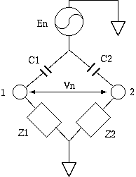
In case of overall shielded twisted pair structure, because shield conductor becomes induced potential source, when degree of balance of capacitance between each conductor and its shield conductor is not good, this cancellation mechanism become not effective so much, therefore it is supervised (controlled) by indicator called Capacitance Unbalance as indicated below. There are some definitions for this Capacitance Unbalance, so the value differs depending on standards. In any case, it is difined that it becomes zero when it is perfectly balanced.
  Cu = 400 * (Ca - Cb) / (2 * (Ca + Cb) - Cc)
  hereby,
	Cu = Capacitance Unbalance (%)
	Ca = Capacitance between Condcutor 1 and Shield while Conductor 2 and Shield are shorted (F/m)
	Cb = Capacitance between Conductor 2 and Shield while Conductor 1 and Shield are shorted (F/m)
	Cc = Capacitance between Conductor and Shield while Conductor 1 and 2 are shorted (F/m)
| Material | σs | μs | σs*μs | σs/μs |
|---|---|---|---|---|
| Copper | 1 | 1 | 1 | 1 |
| Silver | 1.05 | 1 | 1.05 | 1.05 |
| Gold | 0.7 | 1 | 0.7 | 0.7 |
| Aluminum | 0.61 | 1 | 0.61 | 0.61 |
| Brass | 0.26 | 1 | 0.26 | 0.26 |
| Bronze | 0.18 | 1 | 0.08 | 0.08 |
| Tin | 0.15 | 1 | 0.15 | 0.15 |
| Lead | 0.08 | 1 | 0.08 | 0.08 |
| Nickel | 0.2 | 100 | 20 | 2e-3 |
| Stainless Steel (SUS-430) | 0.02 | 500 | 10 | 4e-5 |
| Carbon Steel (SAE 1045) | 0.1 | 1000 | 100 | 1e-4 |
| Super Permalloy (1 kHZ) | 0.03 | 1e5 | 3000 | 3e-7 |
Since the frequency dependence of the magnetic material is extremely large, these value must be seen in the order of reference.